Since the early 1970’s it has been recognized that by accelerating a focused beam of electrons at the surface of a resist, a very high resolution pattern can be produced. This is possible as the wavelength of electrons is smaller than that of the photons of ultra violet radiation by more than three orders of magnitude. This technique is called electron beam lithography or EBL.
EBL is a direct write technique and therefore does not require a mask to be fabricated, it is therefore much more flexible around pattern changes during the development phase of a project, but has the downside of being a slower exposure technique.
To write a pattern into the resist, a computer controlled pattern generator controls the electron beam by deflecting and turning the beam off and on according to a 2D CAD file. Prior to exposure, the CAD file is split into different shapes, which are then pixelated to represent each exposure point of the electron beam, this is called fracturing. The pixilated pattern directs the focused electron beam to exposure locations on the surface of the resist.
A key parameter to consider when developing a EBL exposure is the clearing dose of the resist material. This is defined as the amount of energy that is required to correctly expose the resist material to ensure maximum pattern transfer fidelity. For a positive tone resist this corresponds to the number of electrons that are needed to break all the polymer bonds in the exposed area to clear the resist. For a negative tone resist this corresponds to the number of electrons required to cross-link the resist.
Although many resists state a clearing dose, and some software can model the resists to determine a clearing dose, the most reliable way to determine this is empirically through a dose array test. The variables that affect a clearing dose will be discussed in a later post.
Practically though, to calculate the dose that the electron beam will deposit in the material the following formula is used:
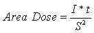
Where I is the probe current of the electron beam, t is the dwell time of the beam (how long the beam will stay at that pixel) and S is the step size (the distance between individual pixels). The area dose in electron beam lithography is typically expressed in µC/cm².
The schematic below shows Monte-Carlo simulations of electron scattering in a PMMA resist layer and the effect of different step sizes on the resist exposure.
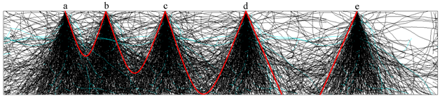
Moving from left to right, the step size increases. It can be clearly observed that although there is only one small area of incidence of the electron beam, the incident electrons scatter laterally, causing the electrons to deposit energy outside of the exposure area. This mechanism is called Proximity Effect. Proximity effect can be used to assist in exposure, but an also hinder the successful pattern exposure.
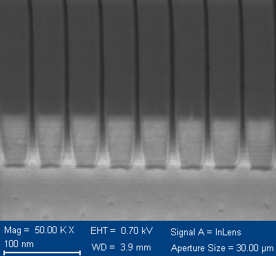
Between incident points A and B, and B and C, the proximity effect aids in the successful exposure of the resist between the pixels, resulting in a correct exposure. However between points C and D, and D and E, the proximity effect is not great enough to fully expose between the pixels. It is therefore essential that a correct step size is selected to ensure a full exposure without over exposure. By extending the dwell time at points D and E, a correct exposure can be achieved, however the scattering occurs in all directions, therefore line widths will inherently increase as well reducing the pattern fidelity. The image below shows lines exposed in SML resist where the proximity effect at the bottom of each line is clearly visible.
A fine balance is required between the step size, dwell time and probe current to successfully expose a patten.